I made some changes to the Arduino sketch to accomodate the larger display (2.8”) and built the project on Vero style strip board.
A special thanks to Jaques VK6KDX for his help with getting the programming procedure into my thick skull.
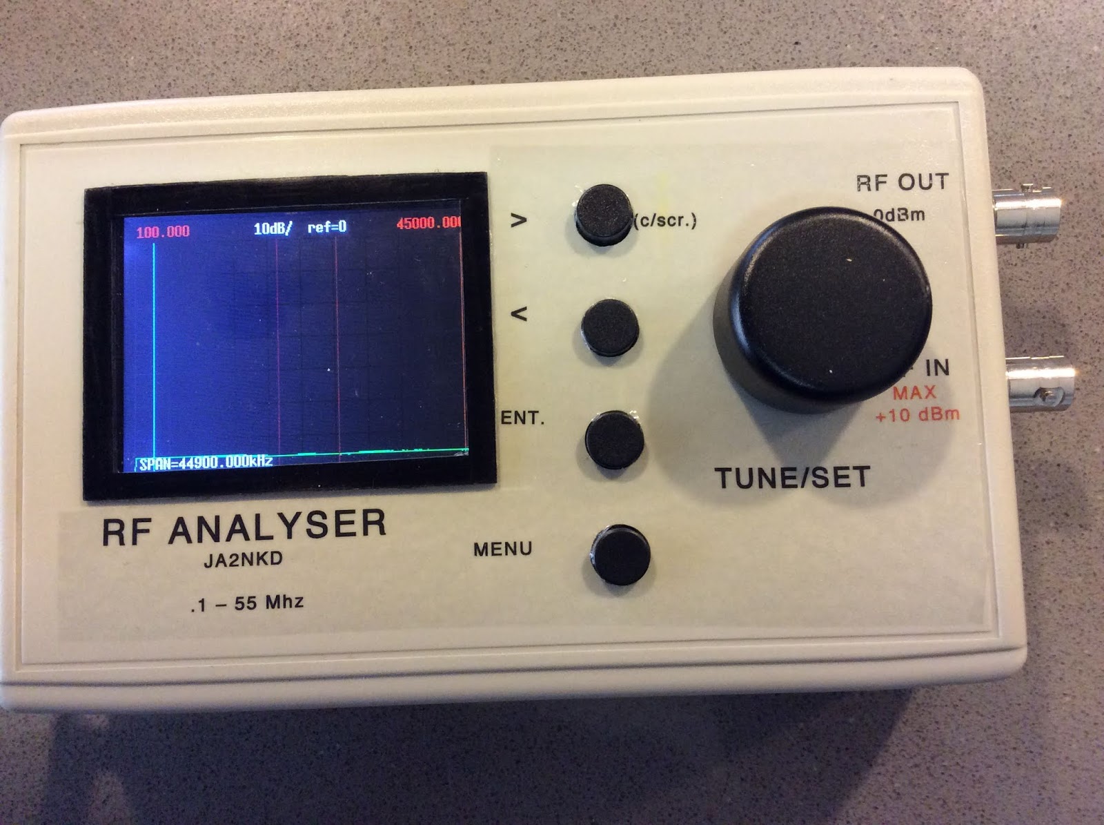
Tuning range is from 1 - 55MHz and includes a signal generator (DDS) with selectable step size, an RF power meter, Scalar network analyser and antenna analyser (with external directional coupler)
A calibration routine for the power meter function is included in the Arduino sketch and once set up, holds good to within 0.1 dB to beyond 148 MHz as compared against my HP8648B signal generator.
It’s important for an instrument of this type to have a clearly defined output impedance of 50 ohms and an output level as close as possible to 0dBm.
The AD9850 DDS evaluation board as standard, comes with an output impedance of 200 ohms with an on board anti alias filter designed around 200 ohms, it has a cut off frequency of around 70 MHz. Another shortcoming of the original module is due to the poor output filter performance, significant 125mhz clock frequency leak through is apparent on the DDS output spoiling the output waveform.
The DDS reference clock is calibrated so that the DDS output is exactly 10 MHz as measured on a frequency counter connected to the output as part of the calibration process and the resulting math is stored within the Arduino EEPROM.
Unfortunately, the sketch uses just about all the included memory capacity in the Arduino NANO
leaving no space to include the usual ‘normalisation’ function to flatten the output frequency response, however, by modifying the AD9850 DDS with a replacement anti alias filter and impedance matching to 50 ohms it is possible to acheive a response that is within +/- 1dB from 100 kHz to 55Mhz.
As an improvement to the original JA2NKD design I have implemented these changes as originally described by Jim Giammanco (N5IB) in his PHSNA design, these changes also result in a gain of some 6db in output level, the new filter is followed by a Pi attenuator that trims to output level to 0dBm. and the 125mhz signal has gone from the output.
Here’s a few photos of the project


Hello,
ReplyDeleteI too am building JA2NKD's analyser and have just got a PCB from India (VU3SXT) https://vu3sxt.blogspot.com/p/rf-analyser.html
The website is somewhat outdated, but basically the same.
I have an analyser running on veroboard and will now transfer it to the PCB for a more elegant layout.
I wonder if you would share your Arduino code and schematics?
I'll try to publish mine as soon as I get it done.
Kind regards,
Nigel - G4ZAL
hello do you have a picture off the balun how to make t62 i belive.
ReplyDeletefor the pcb that vu3sxt has made.
nice case where to buy these?
Wayne,
ReplyDeleteI just finished breadboarding JA2NKD's RF analyzer but can't really figure out the power meter function. Is this designed to measure the power out of the DDS or some input source. Other than that it looks pretty clear and useful.
Thanks, and 73s JACK